

NTNU Physics Team Measures 2 nm Carrier Transfer Length in 2D Transistors
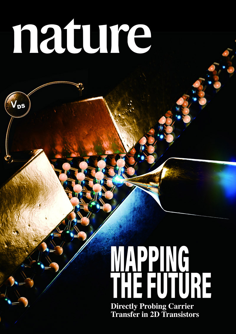
A research team led by Professor Yann-Wen Lan of the Department of Physics at National Taiwan Normal University (NTNU), working with Professor Ya-Ping Chiu’s team at National Taiwan University (NTU) and Professor Lain-Jong Li of the National University of Singapore, who also serves as a Yushan Scholar and visiting chair professor in NTNU’s Department of Physics, has overcome a major bottleneck in contact engineering for two-dimensional (2D) semiconductor transistors. The collaboration achieved the first direct measurement of carrier transfer length in a 2D semiconductor transistor, providing critical experimental evidence for the design of future nanoscale devices. The findings were published in Nature in July 2026, highlighting NTNU’s strengths in 2D semiconductor devices, advanced measurement techniques, and international research collaboration.
As demand for artificial intelligence, high-performance computing, and low-power chips grows rapidly, continued transistor scaling has become a major challenge for the global semiconductor industry. In recent years, atomically thin 2D semiconductors have emerged as leading candidates for extending Moore’s law. Yet scaling the channel is only part of the challenge: the efficiency with which electrons are injected across the metal–semiconductor contact has an equally direct impact on device performance and will be crucial to further scaling.
Lan said the research teams have worked extensively on 2D semiconductor electronic devices and contact engineering. In this study, the NTNU team was responsible for the design, fabrication, and electrical characterization of high-quality 2D semiconductor transistors; Li’s team supplied high-quality 2D materials; and Chiu’s team developed a pioneering operando cross-sectional scanning tunnelling microscopy (STM) technique. The three teams jointly conceived the project, bringing together expertise in material growth, device fabrication, electrical analysis, and atomic-scale measurement to create an integrated interdisciplinary research platform.
The study’s central breakthrough was to directly connect transistor electrical measurements with atomic-scale microscopy for the first time. Previously, carrier transfer length could only be estimated using the conventional transfer length method (TLM), without direct experimental confirmation. By applying bias under actual device operating conditions, the researchers were able to observe electron transport at the edge of the metal–2D-semiconductor contact, and directly measure a carrier transfer length as short as about 2 nanometers. The result demonstrates the potential of 2D semiconductors to continue scaling towards future advanced technology nodes.
Lan noted that the NTNU team established a platform for 2D semiconductor device fabrication, contact engineering, and electrical analysis as part of the study. By testing different device structures and contact designs, the team also developed an important electrical approach for analyzing carrier transfer length. The work not only verifies key physical mechanisms in 2D semiconductor contact engineering, but also establishes a new way to assess contact quality directly, providing valuable guidance for the design of future ultra-scaled transistors.
The operando microscopy technique developed by Chiu’s team could also be extended to silicon devices and other emerging semiconductor materials. It could therefore become a core analytical tool for characterizing contact behavior in a wide range of advanced semiconductor devices, helping accelerate the development of new materials, device architectures, and fabrication processes.
Lan said the study demonstrates NTNU’s research strengths in 2D semiconductor electronics, nanoelectronics, and contact engineering. By combining NTNU’s expertise in 2D-material devices, the international resources made possible through the Yushan Scholar program, and interdisciplinary collaboration with NTU’s atomic-scale measurement team, the researchers were able to deliver a result at the forefront of the field.
The team will continue to pursue research on 2D-material electronic devices, non-volatile memory, optoelectronic devices, and quantum functional materials. The goal is to develop further innovative semiconductor technologies that can provide a foundation for next-generation AI chips, low-power computing, and advanced semiconductor applications.
Source: Yang, ZL., Huang, BC., Lin, YK. et al. Directly probing the carrier transfer length in 2D-material transistors. Nature 655, 350–356 (2026). https://doi.org/10.1038/s41586-026-10707-0
Yann-Wen Lan Distinguished Professor | Department of Physics
Yann-Wen Lan is a professor in the Department of Physics at National Taiwan Normal University and has been recognized by the university as a Distinguished Professor. With support from the National Science and Technology Council and NTNU, his recent research has explored the interaction between the orbital angular momentum of light and two-dimensional materials. His broader research interests include the fundamental physics and practical applications of one-dimensional nanowires and nanotubes, two-dimensional layered materials, and energy-related nanoelectronics.